| Sign In | Join Free | My benadorassociates.com |
|
| Sign In | Join Free | My benadorassociates.com |
|
| Categories | Double Sided PCB |
|---|---|
| Brand Name: | LEFANG |
| Model Number: | RM0002L058 |
| Certification: | ISO9001, ISO14001, ISO/TS16949, SGS, UL, RoHs,OHSAS18000 |
| Place of Origin: | Shenzhen,China |
| MOQ: | 1 Piece |
| Price: | Negotiable |
| Payment Terms: | T/T, Western Union, Paypal, MoneyGram |
| Supply Ability: | 290, 000 sqm Per Month |
| Delivery Time: | 2-10 work days |
| Packaging Details: | Inner: Vacuum Packing; Dry Packing out Packing |
| Raw material: | Fr - 4 |
| Layer count: | 2 Layer |
| Board thickness: | 1.6 mm |
| Copper thickness: | 1 Oz / 35 µm |
| Surface treatment: | OSP |
| Solder mask: | Green |
| Board size: | 124*100 mm |
| Min. Aperture: | 0.3 mm |
| Min. Line Trace Width/Space: | 0.15 / 0.15 mm |
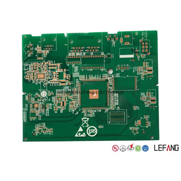
Rigid Double Sided Printed Circuit Board Pcb Double Layer for Automotive Components
The 2 layers double sided PCB is made FR4 substrate material with finish board thickness of 1.6 mm. And it is total specification is 124*100 mm, with green solder mask and OSP surface finish. The double sided PCB is mainly applied to automobile components.
How to get quick quotation?
![]()
| Step 1 Please send us Gerber file with these format: .CAD / .Gerber / .PCB / .DXP / .P-CAD, etc | ||||||||||||||||||||
| Step 2 Also please provide us the below details for quick quotation: | ||||||||||||||||||||
Board material: Fr - 4 / CEM - 1 / CEM - 3 / 22F / Fr - 1 / others | ||||||||||||||||||||
| Material brand: SY / KB / Rogers (optional) | ||||||||||||||||||||
| Material Specification:High Tg / copper based / aluminum based or others (optional) | ||||||||||||||||||||
| Board thickness: 0.1 - 6.0 mm | ||||||||||||||||||||
| Copper thickness: 0.05 Oz - 8 Oz ( 17 um - 288 um ) | ||||||||||||||||||||
| Surface Treatment: OSP / ENIG / HASL / Lead Free HASL / Immersion Tin / Immersion Sin | ||||||||||||||||||||
| Color of solder mask and silk print: Green / red / blue / black / white / yellow ,etc | ||||||||||||||||||||
| Board size and quantity | ||||||||||||||||||||
If you don't have Gerber file, please provide us the imfomation as step 2 or post your PCB Board to us for clone. | ||||||||||||||||||||
SAMPLE: | ||||||||||||||||||||
| ||||||||||||||||||||
| Layer count | Sample lead time/workday | Batch lead time/workday |
| 1-2L | 2 | 6 |
| 4L | 5 | 8 |
| 6L | 5 | 9 |
| 8L | 6 | 10 |
| 10L | 8 | 10 |
| 12L | 8 | 12 |
| 14L | 10 | 15 |
| 16L | 10 | 18 |
| 18-40L (Up to difficulty) | at least 18 | at least 24 |
| P.S. For HDI, Blind/Buried Hole PCB: Regular Lead Time + 3 workdays | ||
-- We have spent massively on purchasing below advanced automated production equipments.
| Equipment Name | Plant in Shenzhen | Plant in Dongguan |
| CCD exposure machine | 8 | 12 |
| AOI test machine | 6 | 8 |
| Mechanical drilling rig | 26 | 53 |
| Automatic edge finishing machine | 2 | 2 |
| Pressing machine | 2 | 2 |
| VCP | 0 | 2 |
| Electroplating line | 1 | 2 |
| CNC routing machine | 12 | 12 |
| Automatic tester | 10 | 16 |
Now send us your inquiry, and you will be replied within 8 hours!
Little knowledge - How to improve the use ratio of PCB Board
1. Enlarge the PCB panel size, the larger panel, the less margin
wasted;
2. Increase the pieces of PCB Board in each Sheet, which could also
decrease the margin waste;
3. If two types of PCB such as A(big) and B(small), they could not
reach a good use ratio when arrayed separately, then you could
consider whether is suitable to array A and B in one sheet;
4. It is great to use professional software to arrange the PCB
Board array.
|
