| Sign In | Join Free | My benadorassociates.com |
|
| Sign In | Join Free | My benadorassociates.com |
|
| Categories | Through Hole PCB Assembly |
|---|---|
| Brand Name: | OEM/ODM |
| Model Number: | SL00710S06 |
| Certification: | UL, Rohs |
| Place of Origin: | China |
| MOQ: | Negotiable |
| Price: | Negotiable |
| Payment Terms: | L/C, T/T, Western Union, MoneyGram |
| Supply Ability: | 5000 Piece/Pieces per Day |
| Delivery Time: | 7-12 days |
| Packaging Details: | ESD Bag |
| Copper thickness: | 1oz,1/2OZ 1OZ 2OZ 3OZ |
| Base material: | Aluminum, FR-4 |
| Min. line spacing: | 4/4mil(0.1/0.1mm) |
| Board thickness: | 0.5~3.2mm |
| Min. line width: | 0.075mm/0.075mm(3mil/3mil) |
| Min. hole size: | 0.20mm,4mil |
| Surface finishing: | HASL,ENIG |
| Product name: | PCB Assembly |
| Application: | Consumer Electronics |
| Pcb assembly method: | SMT |
China Through-hole PCB Assembly free sample Printed Circuit Board Assembly Manufacturer
Through-hole PCBs are employed in many mission-critical electrical assemblies. These PCBs are well-known for the various benefits they offer. SHINELINK Technology Ltd, a leading PCB assembly services are known for manufacturing and providing quality through-hole printed circuit boards. All PCB manufacturing through assembly and packaging is performed by our experienced PCB experts.
We provide through-hole PCB assembly services to meet conventional lead assembly requirements of a variety of industries. We provide single, double-sided, as well as high-density multilayer Plated Through Hole (PTH) circuit board assembly services to meet low to mid volume production requirements of our clients.
PCB Production Capacity
| Layer count | 1-28L,HDI |
| Material | FR-4, High TG FR4, aluminium, FPC |
| Teflon,PTFE (F4B,F4BK), Rogers (4003,4350,5880) | |
| Max board dimensions | 800mm*620mm |
| Board shape | Rectangular,round,slots,cutouts,complex,irregular |
| Board type | Rigid,flexible,rigid-flexible |
| Board cutting | Shear,V-score,tab-routed,counter sunk |
| Board thickness | 0.2~8.0mm, Flex 0.1~0.25mm |
| Thickness Tolerance | ±10% |
| Min line width / space | 3mil/3mil |
| Minimum Drilling Hole (Mechanical) | 0.1mm |
| Minimum laser hole | 0.075mm |
| Blind Hole/buried plate | YES |
| Hole Position/hole Tolerance | PTH:±0.076MM |
| NPTH:±0.05mm | |
| InnerLayer Copper Thickness | 0.5-3 oz |
| OutLayer Copper Thickness | 0.5-4 oz |
| Impedance control tolerance | ±10% |
| Surface finish | HASL,Lead free HASL,ENIG,Immersion Tin,Immersion Silver,OSP... |
| Solder mask | Double-sided green,red,white,blue,black,etc |
| Silkscreen | Double-sided or single-sided in white,black,or negative |
| PCB Testing | E-test, Flying probe test |
| Acceptable File Format | Gerber RS-274X,274D,AutoCAD'S DXF,DWG,Pro-E,Ki-CAD |
| Quality Standards | IPC-A-600F and MIL-STD-105D CHINA GB<4588> |
THT(Wave soldering) process (RoHs Compliant) Capabilities up to:
1.Single side wave soldering
2.SMT & THT mixture process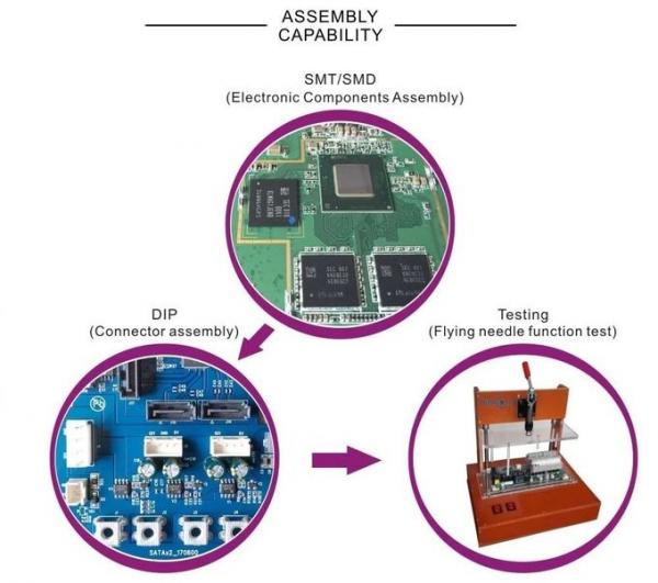
PCB Assembly Capabilities
| Turnkey PCBA | PCB+components sourcing+assembly+package |
| Assembly details | SMT and Thru-hole, ISO lines |
| Lead Time | Prototype: 15 work days. Mass order: 20~25 work days |
| Testing on products | Flying Probe Test, X-ray Inspection, AOI Test, functional test |
| Quantity | Min quantity: 1pcs. Prototype, small order, mass order, all OK |
| Files we need | PCB: Gerber files(CAM, PCB, PCBDOC) |
| Components: Bill of Materials(BOM list) | |
| Assembly: Pick-N-Place file | |
| PCB panel Size | Min size: 0.25*0.25 inches(6*6mm) |
| Max size: 20*20 inches(500*500mm) | |
| PCB Solder Type | Water Soluble Solder Paste, RoHS lead free |
| Components details | Passive Down to 0201 size |
| BGA and VFBGA | |
| Leadless Chip Carriers/CSP | |
| Double-sided SMT Assembly | |
| Fine Pitch to 0.8mils | |
| BGA Repair and Reball | |
| Part Removal and Replacement | |
| Component package | Cut Tape,Tube,Reels,Loose Parts |
| PCB assembly process | Drilling-----Exposure-----Plating-----Etaching & Stripping-----Punching-----Electrical Testing-----SMT-----Wave Soldering-----Assembling-----ICT-----Function Testing-----Temperature & Humidity Testing |
PCBA Picture


|
