| Sign In | Join Free | My benadorassociates.com |
|
| Sign In | Join Free | My benadorassociates.com |
|
| Categories | PCB Manufacturing |
|---|---|
| Brand Name: | CUSTOM MADE |
| Certification: | ISO/UL |
| Place of Origin: | China |
| MOQ: | Negotiable |
| Price: | Negotiable |
| Payment Terms: | T/T |
| Supply Ability: | 100000pc/Month |
| Delivery Time: | 4 Weeks |
| Packaging Details: | PCB + Box |
| Keyword: | PCB Manufacturing |
| PCB Boards: | Thick Copper And Aluminum Boards |
| Features: | Producibility, Testability, Maintainability |
| Applications: | Industrial Control, Medical, Consumer Electronics, PCBA Circuit Board, Electronical Products |
| SMT Capability: | 14 million spots per day |
| Number of layers: | 2-64 layers |
| Materials: | Rogers, Nelco, PTFE, M6, TU862, TU872 |
| Surface Finished: | HASL, HASL Pb Free Immersion Gold/Tin/Silver Osp |
| Payment Method: | T/T |
| Whether to Support customization: | Support |
| Logistics: | Accept customer specified logistics |
| Company Info. |
| TONGZHAN INDUSTRIAL LIMITED |
| View Contact Details |
| Product List |
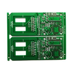
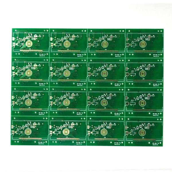
Advanced PCB Manufacturing: Diverse Materials and Precision Processes
PCB Manufacturing Introduction:
Explore our PCB factory's capabilities with a wide range of
insulation materials including FR4, aluminum, copper, ceramic, PI,
and PET. We offer 1 to 12-layer boards with a finished plate
thickness of 0.07mm and above (tolerance +5%/-6%). Inner layer
copper thickness ranges from 18-70μm, and outer layer copper
thickness is 20-140μm.
Experience customization with various solder-resist colors and lettering options and choose from surface treatments like anti-oxidation, immersion gold, and more. Our expertise extends to special processes such as thick copper plating, impedance control, and high-frequency applications. Reinforcement options include FR4, steel, and electromagnetic shielding film.
Our PCBs are designed to fit within a maximum size of 50mm x 100mm, with outer/inner line width and spacing of 0.065mm/3mil. Achieve precision with minimum requirements for solder resist ring width, solder bridge width, solder mask window, and aperture. We maintain an impedance tolerance of 10% and shape tolerance of +0.05mm G laser +0.005mm.
Form your designs using methods like V-cut, CNC, and punching. Join us in shaping the future of electronics with these versatile, precise, and innovative PCB solutions.
PCB Manufacturing Parameters:
| Item | Technical Parameter |
| Layer | 2-64 |
| Thickness | 0.3-6.5mm |
| Copper Thickness | 0.3-12 oz |
| Min Mechanical Hole | 0.1mm |
| Min Laser Hole | 0.075mm |
| HDI | 1+n+1,2+n+2,3+n+3 |
| Max Aspect Ratio | 20:01 |
| Max Board Size | 650mm*1130mm |
| Min Width/Space | 2.4/2.4mil |
| Min Outline Tolerance | ±0.1mm |
| Impedance Tolerance | ±5% |
| Min PP Thickness | 0.06mm |
| Bow &Twist | ≤0.5% |
| Materials | FR4, High-Tg FR4, Rogers, Nelco, RCC, PTFE, M4, M6, TU862, TU872 |
| Surface Finished | HASL, HASL Pb Free Immersion Gold/Tin/Silver Osp, Immersion Gold+OSP |
| Special Capability | Gold Finger Plating, Peelable, Carbon ink |
PCB Manufacturing Process:
1. Gold-plating process: the vertical HASL process is very difficult to flatten very thin pads, which brings difficulty to SMT placement. In addition, the shelf life of the HASL is very short, and gold-plating just solves the problem. these problems.
2. Immersion gold process: The purpose of the immersion gold process is to deposit a nickel-gold coating with stable color, good brightness, flat coating and good solderability on the surface of the printed circuit board. Basically, it can be divided into four stages: pre-treatment (oil extraction, micro-etching, activation, post-immersion), nickel immersion, gold immersion, and post-treatment (waste gold washing, DI washing, drying)
3. Leaded HASL: Leaded eutectic temperature is lower than lead-free, the specific amount depends on the composition of the lead-free alloy, such as the total gold of SNAGCU 217 degrees, the soldering temperature is the eutectic immersion plus 30 degrees or 50 degrees, It depends on the actual adjustment, the lead eutectic is 183 degrees, the mechanical strength, brightness, etc. are better than lead-free.
4. Lead-free HASL: lead will increase the activity of tin wire in the soldering process, lead-tin wire is better than lead-free tin wire, but lead is poisonous, long-term use is not good for human health, and lead-free tin will It is brighter than lead-tin melting, so the solder joint is much stronger.
5. SOP (anti-oxidation): It has anti-oxidation, thermal shock resistance, and corrosion resistance. It is used to protect the copper surface from rusting (oxidation or carbonization) in a normal environment: but in the subsequent welding high temperature, this protection The film must be easily removed quickly by the flux so that the exposed clean copper surface can be melted and soldered immediately in a short time to become a firm solder joint.
PCB Manufacturing Advantages:
1. From PCB proofing to SMT placement, one-stop solution, reducing R&D costs and accelerating product launch.
2. Quick quotation and quick response.
3. The delivery date is fast, and the on-time delivery rate is over 95%
4. Excellent materials, advanced equipment, and strict quality system 5. Exclusive customer service one-to-one service, seamless connection throughout the process

|