| Sign In | Join Free | My benadorassociates.com |
|
| Sign In | Join Free | My benadorassociates.com |
|
| Categories | Indium Phosphide Wafer |
|---|---|
| Brand Name: | ZMSH |
| Model Number: | InAs wafer |
| Place of Origin: | China |
| Payment Terms: | T/T |
| Delivery Time: | 2-4 weeks |
| Material: | Indium Arsenide |
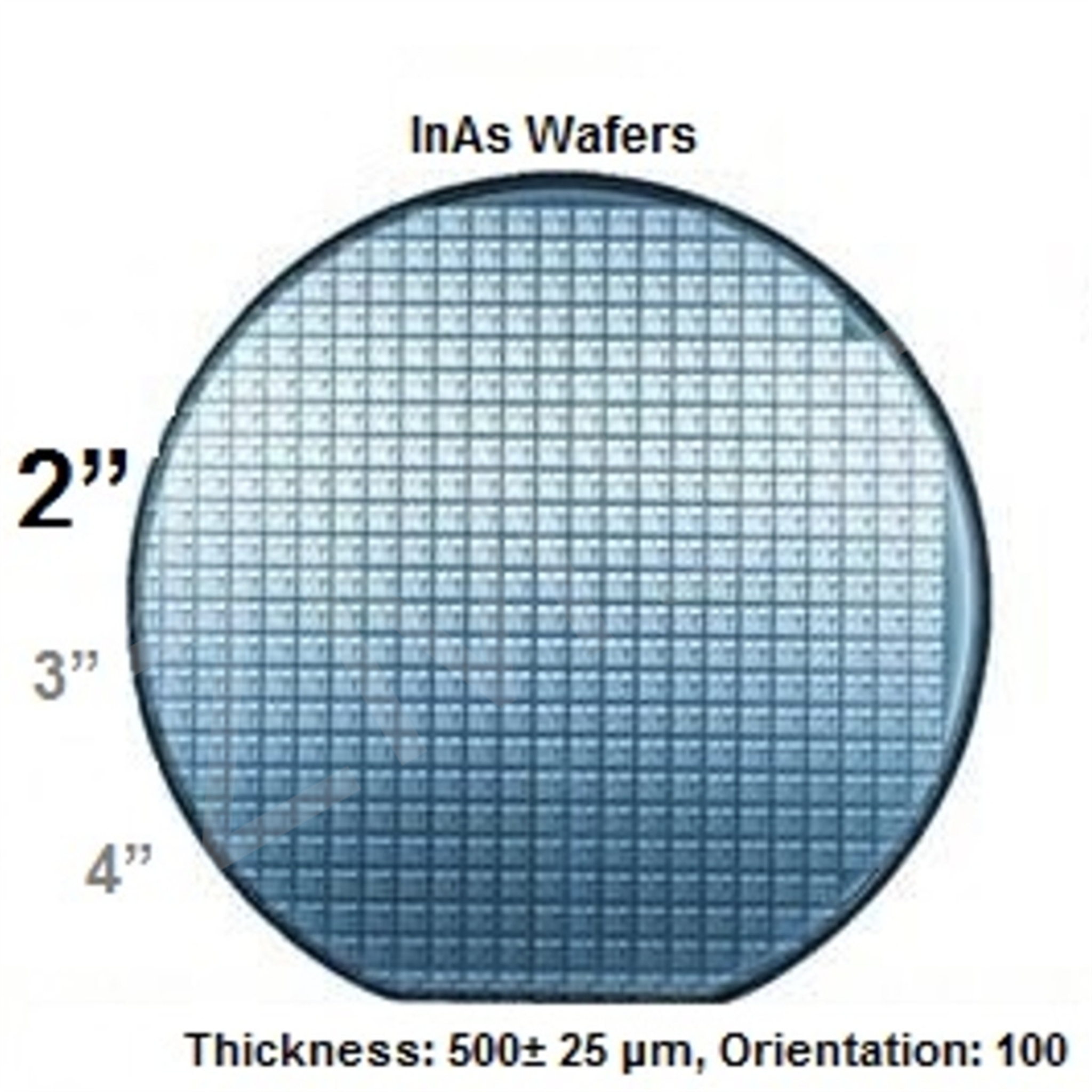
| Size: | 2inch |
| Thickness: | 500um ±25 um |
| Orientation: | <100> |
| Desnity: | 5.67 g/cm |
| Customized: | Supported |
| Company Info. |
| SHANGHAI FAMOUS TRADE CO.,LTD |
| Verified Supplier |
| View Contact Details |
| Product List |
2inch Indium Arsenide Wafer InAs Epitaxial Wafer for LD Laser Diode, semiconductor epitaxial wafer, 3inch InAs-Zn wafer, InAs single crystal wafer 2inch 3inch 4inch InAs-Zn substrates for LD application, semiconductor wafer, Indium Arsenide Laser Epitaxial Wafer
Features of InAs-Zn Wafer
- use InAs wafers to manufacture
- support customized ones with design artwork
- direct bandgap, emits light efficiently, used in lasers.
- in the wavelength range of 1.5μm to 5.6μm, quantum well
structures
- using techniques such as MOCVD or MBE, etching, metallization,
and packaging to achieve the final form of the device
Descriptions of InAs-Zn Wafer
Indium arsenide (InAs) is an important semiconductor material that
is widely used in fields such as infrared detectors and lasers due
to its narrow band gap (about 0.354 eV).
InAs usually exists in the form of a cubic crystal system, and its
high electron mobility makes it perform well in high-speed
electronic devices.
High-quality InAs wafers can be grown through techniques such as
molecular beam epitaxy (MBE) or metal organic chemical vapor
deposition (MOCVD), which can be used to manufacture efficient
infrared detectors, especially in the 3-5 µm and 8-12 µm bands.
In addition, the zinc (Zn) doped InAs structure can adjust its
conductivity to form p-type or n-type semiconductors, thereby
optimizing its electrical properties.
The development of quantum well and quantum dot structures has
further enhanced the application potential of InAs in the
optoelectronic field.
Quantum dot technology enables InAs to play an important role in
emerging fields such as quantum computing and bioimaging.
With the increasing demand for high-performance infrared devices
and quantum technologies, the research and application prospects of
InAs and its doped materials are broad.
Details of InAs-Zn Wafer
| parameter | InAs-ZnWafer |
| Material composition | Indium Arsenic (InAs) +Zinc doping |
| Crystal structure | Cubic system (zinc blende structure) |
| Bandwidth | ~0.354 eV |
| Electron mobility | ~30,000 cm²/V·s |
| Hole mobility | ~200 cm²/V·s |
| density | ~5.67 g/cm³ |
| Melting point | ~942 °C |
| Thermal conductivity | ~0.5 W/m·K |
| Optical band gap | ~0.354 eV |
| Doping method | P Type doping (via zinc) |
| Application Areas | Infrared lasers, detectors, quantum dots |
| Size | Dia 2inch |
| Thickness | 500um ±25um |
| Orientation | <100> |
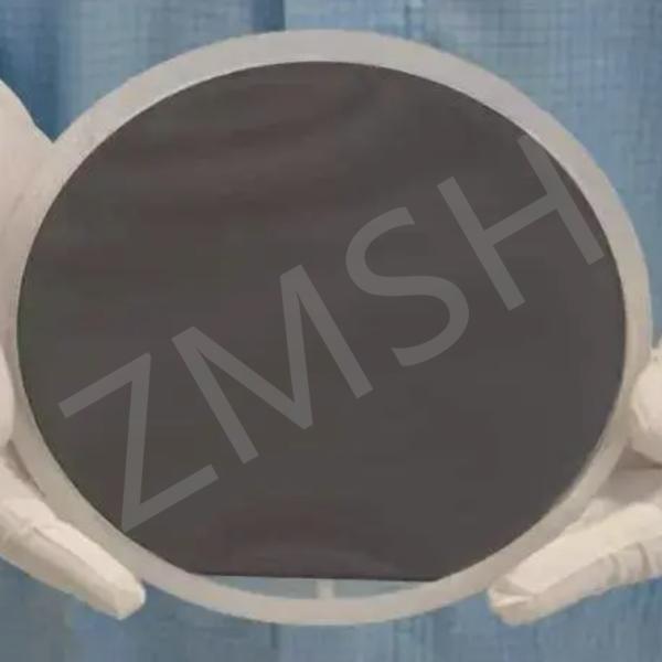
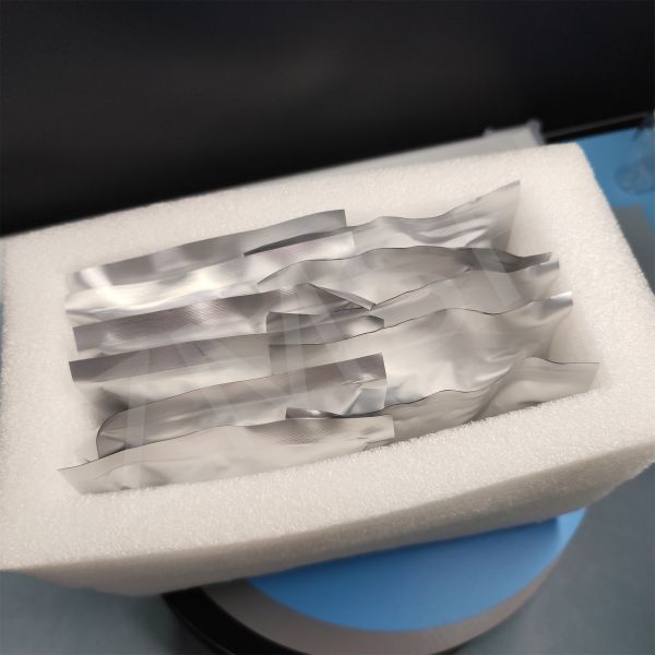
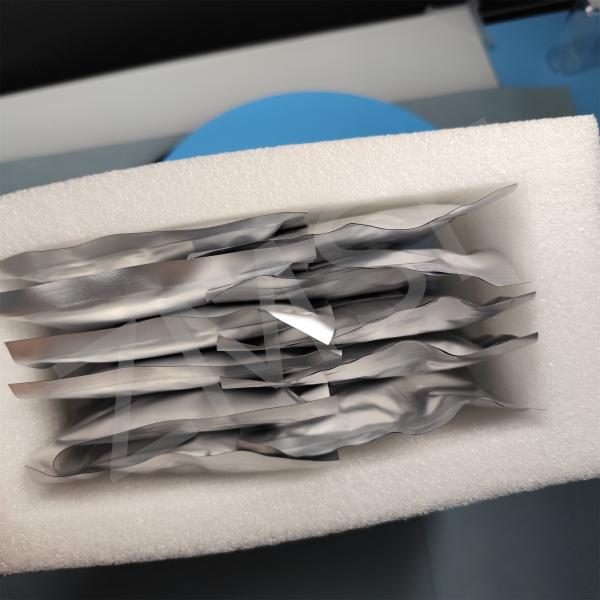
Samples of InAs-Zn Wafer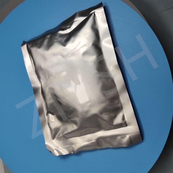
 '
'
*Please feel free to contact us if you have the customized
requirements.
About us
Similar product recommendations
1.2" S
Doped GaP Semiconductor EPI Wafer N Type P Type 250um 300um
Light-Emitting Diodes
2.2" 3" FZ
SiO2 Single Crystal IC Chips 100um 200um Dry Wet Oxidation Layer
100nm 300nm
FAQ
1. Q: What about the cost of InAs-Zn wafers compared with other
wafers?
A: InAs-Zn wafers are typically more expensive than silicon and
GaAs wafers due to material scarcity, complex manufacturing
processes, and specialized market demand.
2. Q: What about the future prospects of InAs-Zn wafers?
A: The future prospects of InAs wafers are quite promising.

|
