| Sign In | Join Free | My benadorassociates.com |
|
| Sign In | Join Free | My benadorassociates.com |
|
| Categories | Fused Quartz Plate |
|---|---|
| Brand Name: | ZMSH |
| Model Number: | 3 Inch Quartz Wafer |
| Certification: | rohs |
| Place of Origin: | CHINA |
| MOQ: | 10 |
| Price: | by case |
| Payment Terms: | T/T |
| Supply Ability: | 1000pcs per month |
| Delivery Time: | 5-8weeks |
| Packaging Details: | Package in 100-grade cleaning room |
| Diameter: | 3 inch (76.2mm) |
| Thickness Tolerance: | ±0.02mm |
| Surface Roughness: | ≤1nm (Polished Grade) |
| Transmittance @193nm: | >92% |
| CTE (RT-300°C): | 0.55×10⁻⁶/°C |
| Applications: | Semiconductor Manufacturing,High-power Lasers |
| Company Info. |
| SHANGHAI FAMOUS TRADE CO.,LTD |
| Verified Supplier |
| View Contact Details |
| Product List |

The 3-inch quartz wafer (76.2mm) is a large-format, high-purity fused silica substrate specifically designed for advanced semiconductor, optoelectronic, and precision optical applications requiring larger processing areas. Compared to 2-inch wafers, the 3-inch specification enhances production efficiency and reduces edge loss, making it particularly suitable for batch-manufactured MEMS devices, advanced photomasks, and laser optical systems.
ZMSH specializes in customized production of large-size quartz wafers, offering:
· Full Size Coverage: From 2-inch to 12-inch wafers, supporting non-standard size customization
· Complex Shape Processing: Round wafers, square plates, and special-shaped cuts (e.g., sector-shaped, D-cut)
· Multi-functional Surface Treatment: Single/double-side polishing, coatings (AR/IR/DLC), micro-structure etching
· Industry Solutions: Semiconductor-grade cleanliness (Class 100), laser drilling, high-precision alignment marks
| Parameter | Specification |
| Diameter | 3 inch (76.2mm) |
| Thickness Tolerance | ±0.02mm |
| Surface Roughness | ≤1nm (Polished Grade) |
| Transmittance @193nm | >92% |
| CTE (RT-300°C) | 0.55×10⁻⁶/°C |
| Parallelism | ≤5μm |
| Vacuum Compatibility | 10⁻⁹ Torr |
- Large-size Homogeneity: TTV≤15μm at 76.2mm diameter ensures process uniformity across large areas
- Deep UV Optimization: >92% transmittance at 193nm, supporting ArF lithography and DUV laser applications
- Thermal Shock Resistance: Thermal expansion coefficient 0.55×10⁻⁶/°C, withstands rapid temperature cycling (1000°C/min)
- Chemical-grade Inertness: Plasma erosion resistant, suitable for dry etching and CMP environments
- Mechanical Reinforcement: Optional chemical strengthening increases flexural strength by 300% to 500MPa
| Field | Specific Applications |
| Semiconductor Manufacturing | Large-format photomask substrates, EUV lithography optics, 3D IC interposers |
| High-power Lasers | Laser resonator mirrors, kW-level fiber laser end caps, ultrafast laser pulse compression grating substrates |
| Quantum Technology | Qubit carrier wafers, cold atom chip vacuum viewports |
| Aerospace | Satellite optical payload windows, radiation-resistant sensor protection covers |
| Biomedical | Microfluidic chip masters, DNA sequencing chip substrates, endoscope light guides |
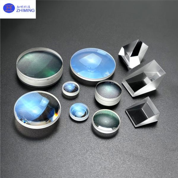
ZMSH provides quartz prism customization services for UV to IR wavelengths, including right-angle prisms, pentaprisms, and beam splitter prisms, featuring:
· Nanometer-level Surface Accuracy (λ/10@632.8nm)
· Special Coatings (laser damage-resistant coatings, polarizing beam splitter coatings)
· Integrated Processing (prism-wafer hybrid structures, microchannel cooling designs)
Ideal for cutting-edge applications in laser beam shaping, spectral analysis, and high-energy physics experiments.

1. Q: What are the advantages of 3-inch quartz wafers over smaller sizes?
A: 3-inch (76.2mm) quartz wafers provide 44% more usable area than 2-inch wafers, reducing edge loss and increasing throughput for MEMS manufacturing and optical coating processes.
2. Q: How to handle and store 3-inch fused silica wafers properly?
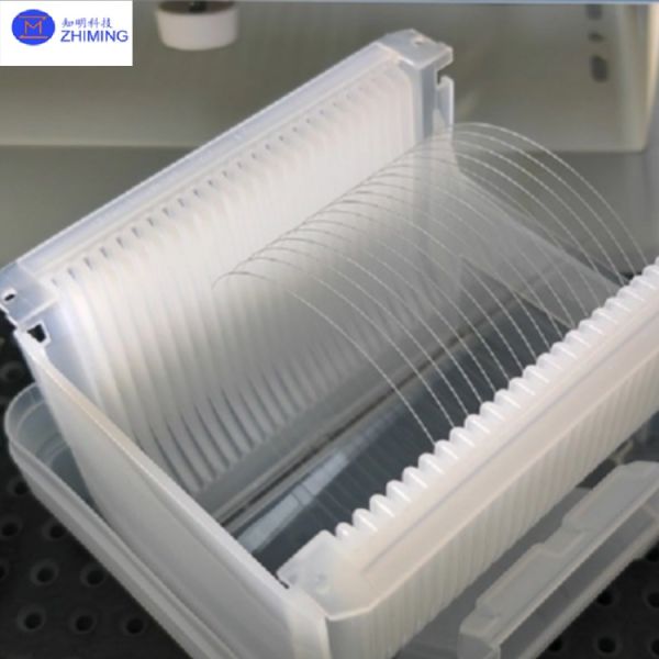
A: Always use cleanroom-grade wafer carriers with edge-contact supports, and store in Class 100 environments with <40% RH to prevent surface contamination and moisture absorption.
Tag: #3 Inch Quartz Substrate, #Customized, #Fused Silica Plates, #SiO₂ Crystal, #Quartz wafers, #JGS1/JGS2 Grade, # High-Purity, #Fused Silica Optical Components, #Quartz Glass Plate, #Custom-Shaped Through-Holes, #3 Inch Quartz Substrate, #76.2mm Diameter

|
