| Sign In | Join Free | My benadorassociates.com |
|
| Sign In | Join Free | My benadorassociates.com |
|
| Categories | HDI and BGA PCBs |
|---|---|
| Brand Name: | PCBgate |
| Model Number: | 262004005 |
| Certification: | ISO9001/UL/ISO14001/IATF16949/RoHS |
| Place of Origin: | China |
| MOQ: | 1 pc |
| Price: | 1-2$ |
| Payment Terms: | L/C,D/A,D/P,T/T,Western Union |
| Supply Ability: | 10000pcs/2 days |
| Delivery Time: | 7 work days |
| Packaging Details: | Vacum Packing |
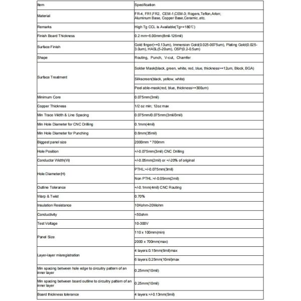
| Base Material: | FR-4 |
| Layer Count: | 1-20 Layers |
| Board Thickness: | 0.2mm-6mm |
| Copper Thickness: | 0.5oz-12oz(18μm - 420μm) |
| Surface Finish: | HASL/ENIG(Gold)/OSP/Immersion Gold |
| Solder Mask: | Green/White/Red/Blue/Black |
| Silkscreen: | White/Black/Yellow |
| Min. Hole Size: | 0.1mm(CNC Drilling) / 0.6mm (Punching) |
| Min. Trace Width/Space: | 3 mil/3 mil (0.075mm) |
| Testing: | Electrical Test |
| Impedance Control: | Available |
| Company Info. |
| SHENZHEN PCBGATE GROUP Co.,Ltd. |
| Verified Supplier |
| View Contact Details |
| Product List |
6-Layer HDI Antenna PCB: High-Frequency RF Signal Interconnect
Product Overview:
Our 6-layer HDI Antenna PCBs are precision-engineered for the demands of high-frequency wireless communication, including 5G, satellite positioning, and MIMO arrays. By integrating advanced 2+N+2 laser micro-via structures, we enable ultra-dense routing while maintaining dedicated shielding layers to eliminate signal crosstalk. These boards feature high-stability dielectric materials with low Dk/Df properties, ensuring maximum gain and minimal transmission loss. Designed for compact RF modules and telecommunications hardware, our HDI solution delivers the high-speed performance and signal purity essential for modern connected devices.
Key Selling Points:
• High Gain: Optimized 6-layer stack-up for maximum RF signal reach.
• Low Loss: High-frequency materials ensure minimal signal attenuation.
• Anti-Interference: Advanced HDI shielding for pure data transmission.


Engineering Support: DFM (Design for Manufacturing) check before production.

Testing: Flying Probe Test, Fixture Test, Impedance Control Test, Thermal Stress Test.
“ Instant PCB(1-38 layers)”--PCBgate
PCBgate is a professional PCB manufacturer providing high-quality printed circuit boards for global electronics industries.
We are capable of manufacturing a wide range of PCB types to meet different application requirements, including:FR-4 PCBs,ceramic PCBs,carbon oil PCBs,Aluminum PCBs,Flexible & Rigid-Flex PCBs.

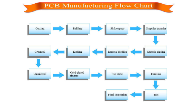
We specialize in 6-layer HDI Antenna PCB manufacturing, providing the perfect balance between multi-band signal isolation and space efficiency. By using Laser Direct Imaging (LDI) and high-speed laser drilling, we achieve the precise registration required for your advanced RF impedance and phased-array designs.
This 6-layer structure is ideal for 5G base stations, satellite terminals, and smart IoT gateways. We ensure 100% E-test and AOI inspection to guarantee that every board meets the highest industrial standards for signal stability and performance.
We support HDI PCB prototypes, small-batch production, and mass production to meet different customer requirements, helping you accelerate your product's time-to-market.
Our PCB manufacturing capability includes:
• Fine Line Technology: Min. Trace/Space down to 0.075mm / 0.075mm
• Blind & Buried Vias: Professional via-in-pad and resin filling processes
• High-End Materials: High-TG, Low-Loss, and Halogen-free laminates
• Surface Finishes: ENIG, ENEPIG, and OSP for superior soldering
• Complex Stack-ups: Multilayer HDI integration up to 20+ layers
• Rigorous Testing: AOI, Micro-sectioning, and Impedance Control

Attention: pictures are for reference only. The specific products are subject to the original factory model.


Standard Packaging: Inner Vacuum Packaging + Outer Carbon Box.
Delivery Partners: EMS,DHL,SF-express, FedEx, UPS or Sea/Air Freight for bulk orders.

• 15 years of experience in PCB manufacturing.
• Advanced Equipment: Equipped with high-speed CNC drilling machines and AOI testing lines.
• Professional engineering support
• Fast prototype delivery
• Global customers from Europe, USA and Asia
• Own Global Supply System.
• Fast and safe way by EMS/DHL/SF-express/Fedex,etc.
• New styles updating everyday and MOQ for all the styles;

1. What's your MOQ and what is PCBgate's fastest delivery time?
A: Our MOQ is Minimum packaging quantity, please contact us for details. Sample to mass production all can be supported by PCBgate.
2. Which payment terms does PCBgate accept?
A:Advance T/T,Western Union,Paypal, L/C,Credit Card, Cheque,Money Gram and Others.
3.What files are required for PCB quotation?
A:Gerber files, PCB specifications and quantity.
4. How to test PCB boards?
A: AOI, Fly probe testing, Text fixture testing, FOC etc. For bare PCB.
Shipping Information
| FOB Port Shenzhen | Lead Time 7-15 days |
| Weight per Unit 1.0 Kilograms | Dimensions per Unit 7.2x3.2x0.06 Centimeters |
| HTS Code 8517.79.90 00 | Units per Export Carton 36.0 |
| Export Carton Dimensions L/W/H 58.0x26.0x36.0 Centimeters | Export Carton Weight 0.1 Kilograms |
Welcome to send us your PCB Gerber files for quotation.
Our engineering team will respond within 24 hours.

|
