| Sign In | Join Free | My benadorassociates.com |
|
| Sign In | Join Free | My benadorassociates.com |
|
| Categories | Semiconductor Equipment |
|---|---|
| Brand Name: | ZMSH |
| Model Number: | Wafer Bonding Equipment |
| Certification: | rohs |
| Place of Origin: | CHINA |
| MOQ: | 2 |
| Price: | by case |
| Payment Terms: | T/T |
| Delivery Time: | 5-10months |
| Bonding Methods:: | Room Temperature Bonding |
| Compatible Wafer Sizes:: | ≤12 Inch, Compatible With Irregular Shaped Samples |
| Compatible Materials:: | Sapphire, InP, SiC, GaAs, GaN, Diamond, Glass, Etc |
| Max Pressure Of Press System:: | 100 KN |
| Alignment Method & Precision:: | Edge alignment accuracy: ≤±50 μm; Mark alignment accuracy: ≤±2 μm |
| Bonding Strength:: | ≥2.0 J/m² @ room temperature (for Si-Si direct bonding) |
| Company Info. |
| SHANGHAI FAMOUS TRADE CO.,LTD |
| Verified Supplier |
| View Contact Details |
| Product List |
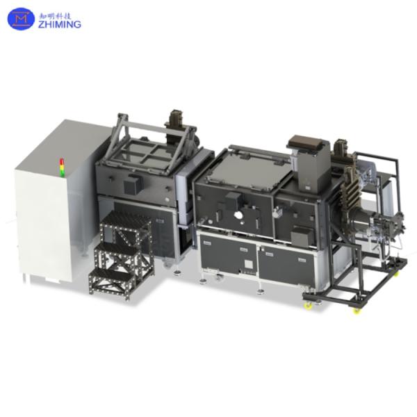
Wafer Bonding Equipment Room Temperature Bondin Hydrophilic Bonding Si-SiC Si-Si Bonding 2 -12 inch
Wafer Bonding System Overview
Wafer Bonding Equipment is a high-end bonding equipment specifically designed for silicon carbide (SiC) power device manufacturing, supporting 2 to 12-inch wafer specifications. Wafer Bonding Equipment incorporates advanced room-temperature direct bonding and surface-activated bonding technologies, with special optimization for SiC-SiC and SiC-Si heterogeneous bonding processes. Featuring an integrated high-precision optical alignment system (≤±2 μm) and closed-loop temperature/pressure control, it ensures the high bonding strength (≥2 J/m²) and superior interface uniformity required for power semiconductor device fabrication.
Wafer Bonding System Technical Specifications
Core Functional Parameters:
| Bonding Processes: | Supports direct bonding and plasma-activated bonding |
| Wafer Compatibility: | Full-range 2"-12" wafer handling |
| Material Combinations: | Si-SiC/SiC-SiC heterostructure bonding |
| Alignment System: | Ultra-high precision optical alignment (≤±0.5 μm) |
| Pressure Control: | Precision adjustable 0-10 MPa |
| Temperature Range: | RT-500°C (optional preheat/annealing module) |
| Vacuum Level: | Ultra-high vacuum environment (≤5×10⁻⁶ Torr) |
Intelligent Control System:
· Industrial-grade touch HMI
· ≥50 stored process recipes
· Real-time pressure-temperature closed-loop feedback
Safety Protection System:
· Triple interlock protection (pressure/temperature/vacuum)
· Emergency braking system
· Class 100 cleanroom compatibility
Extended Functions:
· Optional robotic wafer handling
· SECS/GEM communication protocol support
· Integrated inline inspection module
Wafer Bonding Equipment is specifically designed for R&D and mass production of third-generation semiconductors. Wafer Bonding Equipment modular architecture enables high-reliability bonding for SiC-based power devices. The innovative plasma pretreatment technology significantly enhances interfacial bonding strength (≥5 J/m²), while the ultra-high vacuum environment ensures contaminant-free bonding interfaces. The intelligent temperature-pressure control system, combined with submicron alignment accuracy, provides wafer-level bonding solutions for HEMT, SBD and other devices.
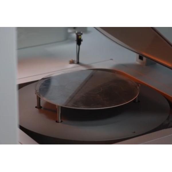
Photo
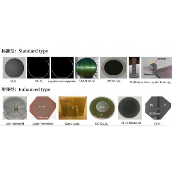
Compatible Materials
Applications
· MEMS Device Packaging: Wafer Bonding Equipment is suitable for hermetic sealing of microelectromechanical systems (MEMS) such as accelerometers and gyroscopes.
· CIS Image Sensors: Wafer Bonding Equipment enables low-temperature bonding between CMOS wafers and optical glass substrates.
· 3D IC Integration: Wafer Bonding Equipment supports room-temperature stacking bonding for through-silicon via (TSV) wafers.
· Compound Semiconductor Devices: Wafer Bonding Equipment facilitates epitaxial layer transfer for GaN/SiC power devices.
· Biochip Fabrication: Wafer Bonding Equipment provides low-temperature packaging solutions for microfluidic chips.
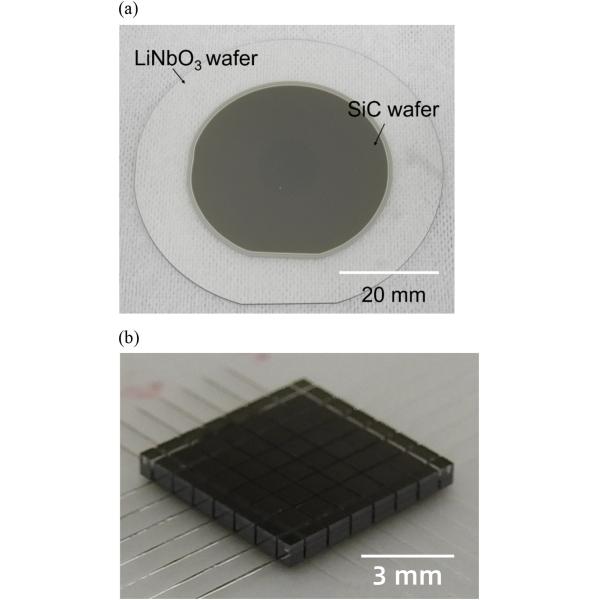
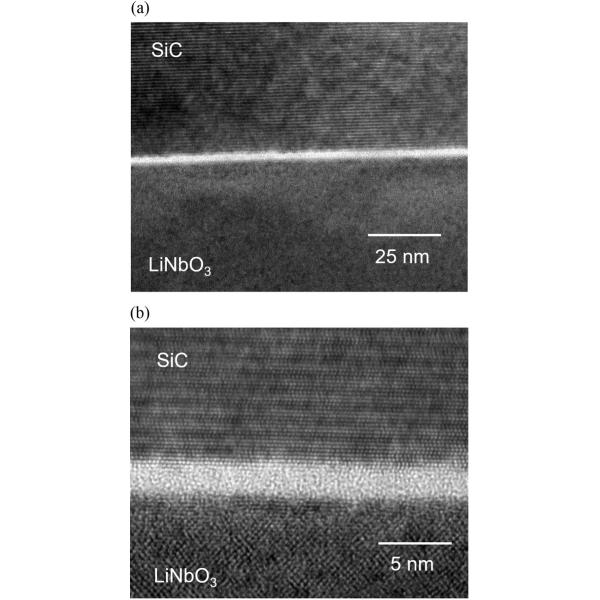
Machining effect——Bonding of LiNbO 3 wafer and SiC wafer
( (a) Photograph of LiNbO3/SiC wafers bonded at room temperature. (b) Photograph of diced 1 × 1 mm chips. )
( (a) Cross-sectional TEM image of the LiNbO₃/SiC bonding interface (b) Magnified view of (a) )
Q&A
1. Q: What are the advantages of room-temperature wafer bonding
compared to thermal bonding?
A: Room-temperature bonding prevents thermal stress and material
degradation, enabling direct bonding of dissimilar materials (e.g.,
SiC-LiNbO₃) without high-temperature limitations.
2. Q: Which materials can be bonded using room-temperature wafer
bonding technology?
A: It supports bonding of semiconductors (Si, SiC, GaN), oxides
(LiNbO₃, SiO₂), and metals (Cu, Au), ideal for MEMS, 3D ICs, and
optoelectronic integration.
Tag: #Wafer Bonding Equipment, #SIC, #2/4/6/8/10/12 inch Bonding,
#Room Temperature Bonding System, # Si-SiC , # Si-Si, #LiNbO 3 -SiC
|
