| Sign In | Join Free | My benadorassociates.com |
|
| Sign In | Join Free | My benadorassociates.com |
|
| Categories | SiC Substrate |
|---|---|
| Brand Name: | ZMSH |
| Model Number: | 4inch SiC Epitaxial Wafer |
| Certification: | rohs |
| Place of Origin: | CHINA |
| MOQ: | 10 |
| Price: | by case |
| Payment Terms: | T/T |
| Supply Ability: | 1000pcs per month |
| Delivery Time: | 5-8weeks |
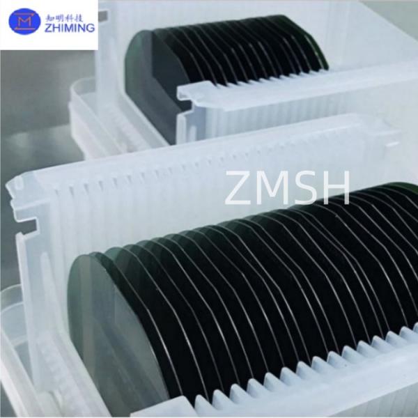
| Packaging Details: | Package in 100-grade cleaning room |
| Crystal Structure: | 4H-SiC single crystal |
| Size: | 4inch |
| Diameter: | 100 mm (±0.1 mm) |
| Doping Type: | N-type/P-type |
| Thickness: | 350μm |
| Edge Exclusion: | 3 mm |
| Company Info. |
| SHANGHAI FAMOUS TRADE CO.,LTD |
| Verified Supplier |
| View Contact Details |
| Product List |
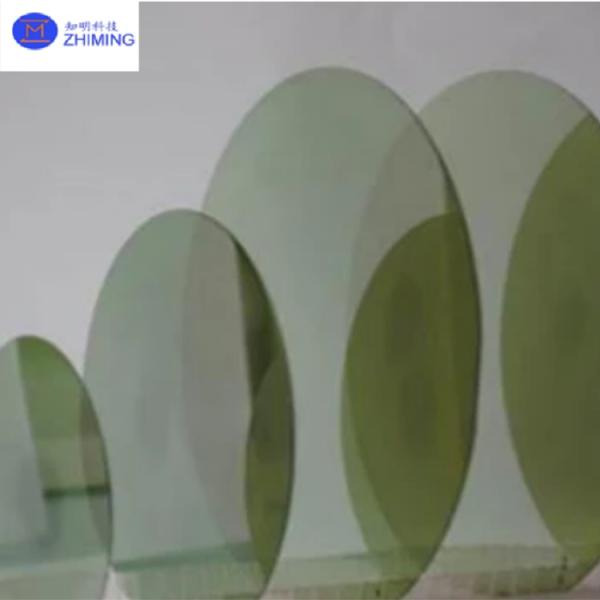
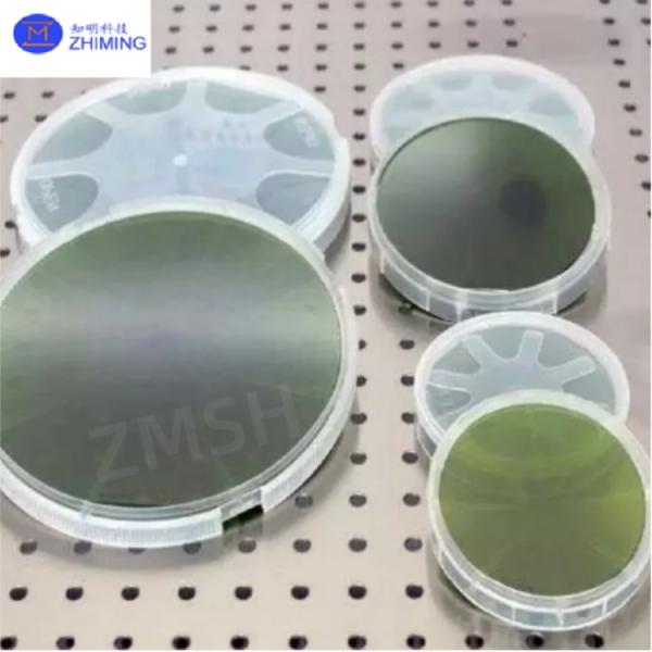
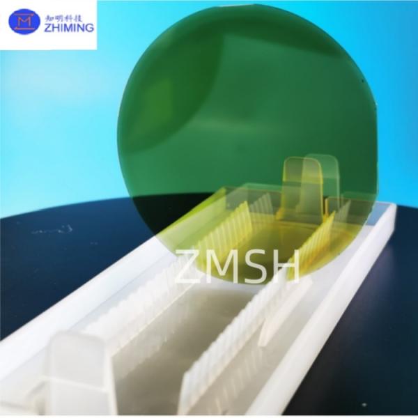
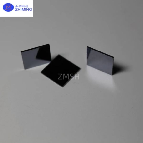
4inch SiC Epitaxial Wafer 4H-N Diameter 100mm Thickness 350μm Prime Grade
As a core material for silicon carbide (SiC) power device manufacturing, the 4-inch SiC epitaxial wafer is based on a 4H-N-type SiC wafer, grown using chemical vapor deposition (CVD) to produce a high-uniformity, low-defect-density single-crystal thin film. Its technical advantages include:
· Crystal Structure: (0001) silicon-face orientation with a 4° offcut to optimize lattice matching and reduce micropipe/stacking fault defects.
· Electrical Performance: N-type doping concentration precisely controlled between 2×10¹⁴–2×10¹⁹ cm⁻³ (±14% tolerance), achieving resistivity adjustable from 0.015–0.15 Ω·cm via in-situ doping technology.
· Defect Control: Surface defect density <25 cm⁻² (TSD/TED), triangular defect density <0.5 cm⁻², ensured by magnetic-field-assisted growth and real-time monitoring.
Leveraging domestically developed CVD equipment clusters, ZMSH achieves full-process control from wafer processing to epitaxial growth, supporting rapid small-batch trials (minimum 50 wafers) and customized solutions for applications in new energy vehicles, photovoltaic inverters, and 5G base stations.
| Parameter | Specification |
| Diameter | 100 mm (±0.1 mm) |
| Thickness | 10–35 μm (low voltage) / 50–100 μm (HV) |
| Doping Concentration (N) | 2×10¹⁴–2×10¹⁹ cm⁻³ |
| Surface Defect Density | <25 cm⁻² (TSD/TED) |
| Resistivity | 0.015–0.15 Ω·cm (adjustable) |
| Edge Exclusion | 3 mm |
1. Material Performance
- Thermal Conductivity: >350 W/m·K, ensuring stable operation at >200°C, 3× higher than silicon.
- Breakdown Field Strength: >3 MV/cm, enabling 10kV+ high-voltage devices with optimized thickness (10–100 μm).
- Carrier Mobility: Electron mobility >900 cm²/(V·s), enhanced by gradient doping for faster switching.
2. Process Advantages
- Thickness Uniformity: <3% (9-point test) via dual-temperature zone reactors, supporting 5–100 μm thickness control.
- Surface Quality: Ra <0.5 nm (AFM), optimized by hydrogen etching and chemical mechanical polishing (CMP).
- Defect Density: Micropipe density <1 cm⁻², minimized through reverse-bias annealing.
3. Customization Capabilities
- Crystal Orientation: Supports (0001) silicon-face, (11-20) carbon-face, and quasi-homoepitaxial growth for trench MOSFETs and JBS diodes.
- Packaging Compatibility: Offers double-sided polishing (Ra <0.5 nm) and wafer-level packaging (WLP) for TO-247/DFN.
1. New Energy Vehicles
- Main Drive Inverters: 1200V epitaxial wafers for SiC MOSFET
modules, improving system efficiency to 98% and reducing EV range
loss by 10–15%.
- Fast Charging: 600V wafers enabling 800V platforms for
30-minute 80% charging (e.g., Tesla, NIO).
2. Industrial & Energy
- Solar Inverters: 1700V wafers for DC-AC conversion, boosting
efficiency to 99% and lowering LCOE by 5–8%.
- Smart Grids: 10kV wafers for solid-state transformers (SST),
reducing transmission losses to <0.5%.
3. Optoelectronics & Sensing
- UV Detectors: Utilizing 3.2 eV bandgap for 200–280 nm
detection in flame monitoring and biochemical threat detection.
- GaN-on-SiC RF Devices: HEMTs on 4-inch wafers for 5G base
stations, achieving 70% PA efficiency.
4. Railway & Aerospace
- Traction Inverters: High-temperature wafers (-55°C–200°C) for
IGBT modules in bullet trains (AEC-Q101 certified).
- Satellite Power: Radiation-hardened wafers (>100 krad(Si))
for deep-space DC-DC converters.
1. Core Competencies
· Full-Size Coverage: 2–12-inch SiC substrates/epitaxial
wafers, including 4H/6H-N, HPSI, SEMI, and 3C-N polytypes.
· Custom Fabrication: Custom cutting (through-holes, sectors),
double-side polishing, and WLP.
· End-to-End Solutions: CVD epitaxy, ion implantation,
annealing, and device validation.
2. Production Capacity
· 6-inch Wafers: 360,000 annual capacity; 8-inch R&D line
operational.
· Certifications: IATF 16949-certified, >95% yield for
automotive-grade products.
· Cost Leadership: 75% domestic CVD equipment, 25% lower costs
vs. international competitors.
The following is the recommended 3C-N type for SiC substrates:
1. Q: What are the key advantages of 4-inch SiC epitaxial wafers?
A: High uniformity (<3% thickness variation) and ultra-low defect density (<0.5 cm⁻² triangles) enable reliable performance in high-voltage (10kV+) and high-temperature (>200°C) power devices.
2. Q: Which industries use 4-inch SiC epitaxial wafers?
A: Primarily automotive (EV inverters, fast charging), renewable energy (solar inverters), and 5G communications (GaN-on-SiC RF devices).
Tags: #4inch, #Customized, #Diameter 100mm, #4H-N Type, # SiC Epitaxial Wafer, #High-Temperature Sensors, #Silicon carbide, #Thickness 350μm, #Prime Grade

|
